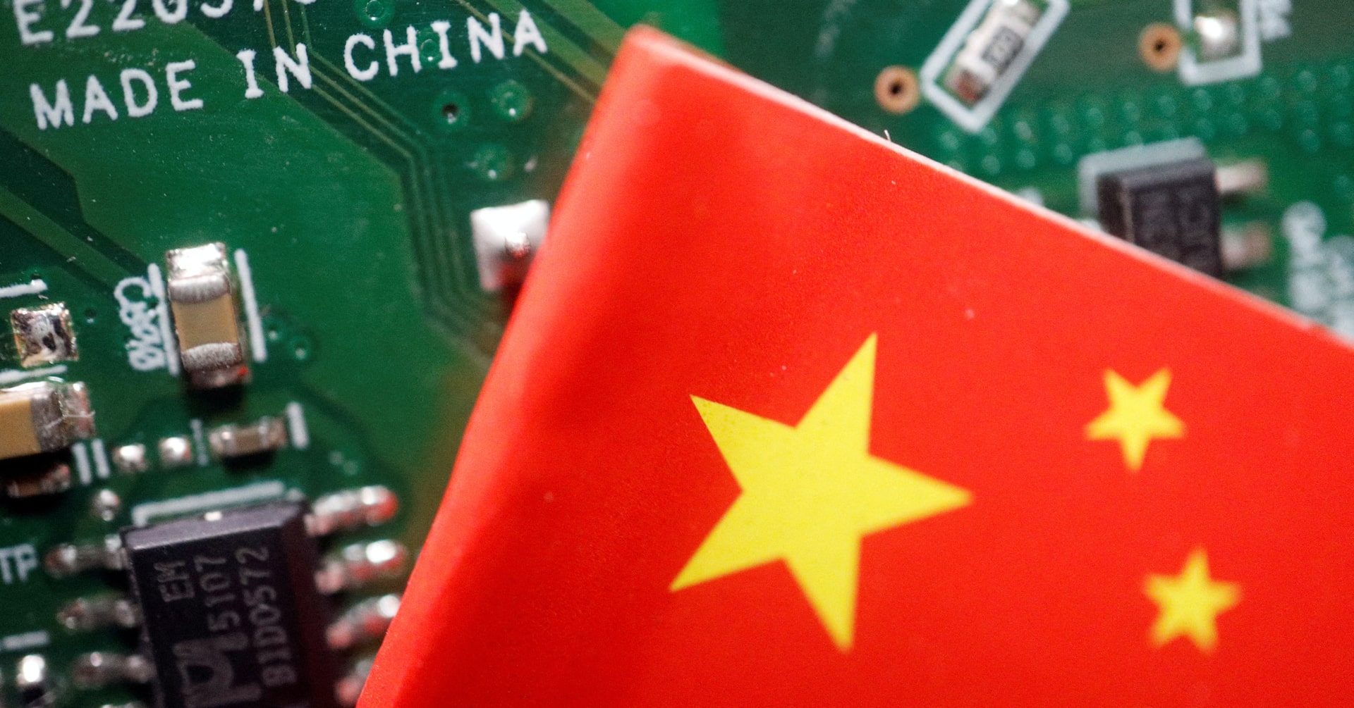
Report: China’s “Manhattan Project” built an advanced EUV chip fab prototype
The most advanced chipmaking process in the world is currently owned by one company: Dutch chipmaker ASML.
The process, known as extreme ultraviolet lithography (EUV), allows for the smallest, most complex semiconductors to be etched onto silicon chips.
These advanced chips are used in a huge number of crucial industries such as AI, mobile phones, and weapons manufacturing.
A new report from Reuters says that China has completed a factory-sized prototype of an EUV chip fab, a first that could have huge ramifications for the balance of power in the global technology race.
The prototype was built in a high-security facility in Shenzhen by former ASML employees and made use of secondary markets to acquire older, used ASML parts, according to the report. Despite a goal of delivering working chips by 2028, sources say China is likely a couple years behind that schedule.
ASML’s $250 million EUV machines are used to manufacture advanced chips for Nvidia, Advanced Micro Devices, and for chips made by TSMC.
ASML shares were down about 4.8% as of 12 p.m. ET.